In the nanocrystal device development process, engineers conduct multiple experiments before making final products. Each experiment requires a long time (more than half a day, including preparation) and is expensive (more than a hundred dollars), making it difficult to use a comprehensive experiment planning method such as “Experimental Design” or “Taguchi methods”. Therefore, in this trial and error process, the engineers modify experimental parameters step by step.
In this planning process, skilled engineers give advice to other engineers in two formats. One is direct advice that shows how to modify these parameters. The other is indirect advice that suggests that the user should read related experiment records.
For the first step of our project, we have built an experiment record management system that supports the search for useful experiment records from the available records.
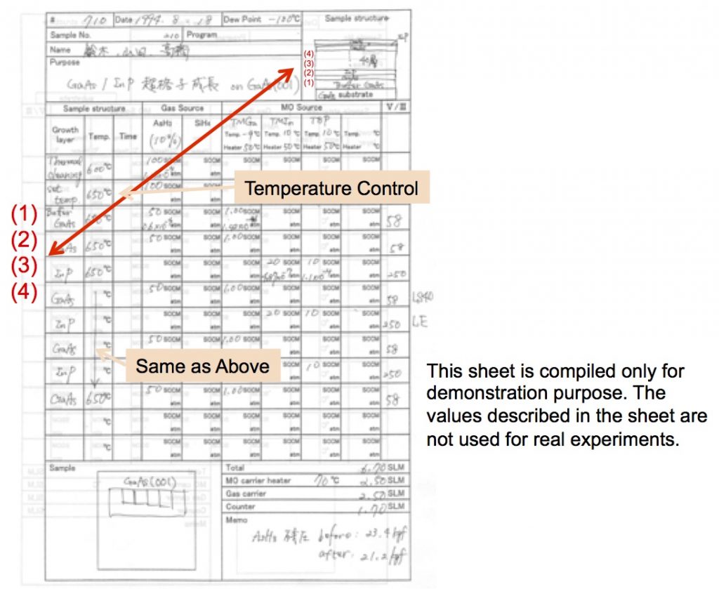
Example of Experiment Record Sheet
We have implemented a prototype system for the SA-MOVPE experiment record management system. This system has an interface that is similar to the image of the original sheet.
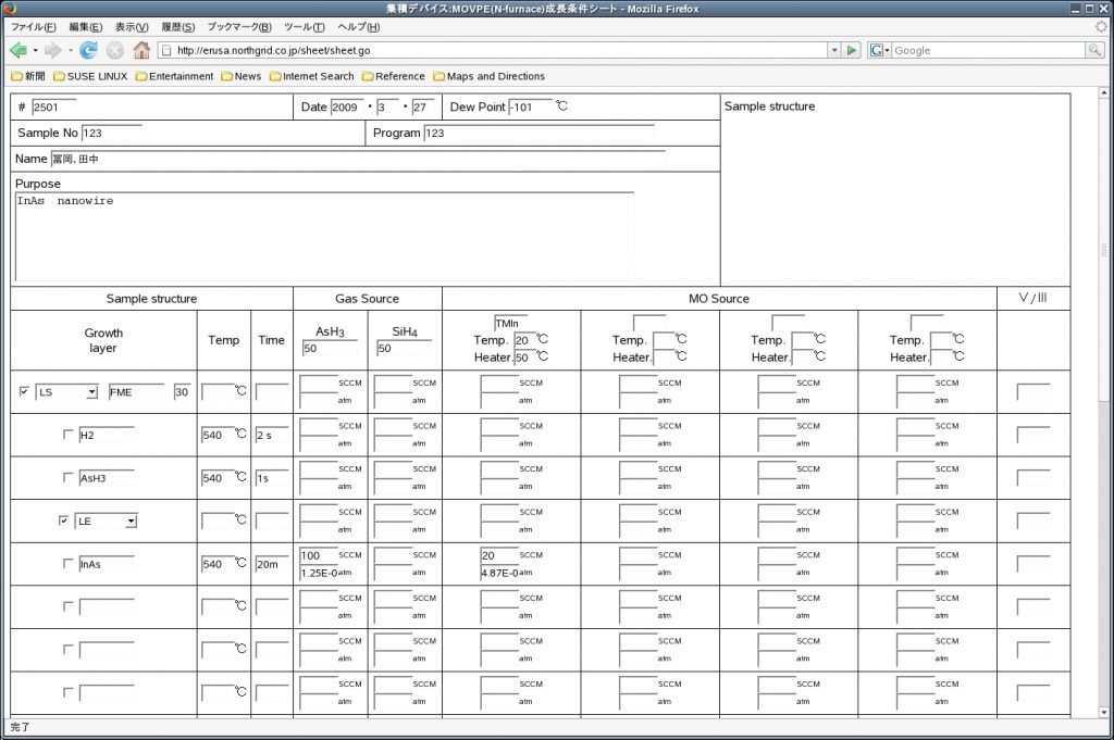
In this system, we can store all the information of the original sheet except diagrams. In addition, this system can use structured queriesbased on the XML data (e.g., find records that have the name “Tomioka” as experimenter, find records that have a layer “p-GaAs” on a layer “p-AlGaAs”).
This system has following functions.
- Frequent-item mining
In the XML record of each experiment, there are several routine descriptions. Therefore, simple frequent-pattern mining may find such information, even though it may be very difficult to analyze the results. We therefore implement simple frequent-item enumeration for the records that match particular conditions (e.g., records for a particular growth layer). - Parametric information visualization
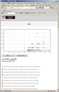
The system uses an interactive parametric information visualization system to form groups for comparison (Figure \ref{fig:system2}). By using this framework, the user can understand the relationship between two different parameters and the frequency associated with the label (e.g., name of the layer).
- Masaharu Yoshioka, Katsuhiro Tomioka, Shinjiroh Hara, and Takashi Fukui : Knowledge Exploratory Project for Nanodevice Design and Manufacturing. In iiWAS ’10 Proceedings of the 12th International Conference on Information Integration and Web-based Application & Services, pp. 871–874 , 2010.