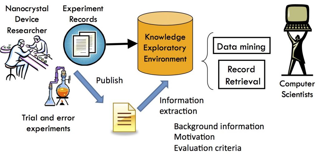
“Knowledge exploratory project for nanocrystal device development” aims to support this knowledge transfer process. This project is one of the real use cases based on collaboration between nanocrystal device engineers and computer science researchers.
The nanocrystal device development process is not well systematized, and it requires both engineering knowledge and craftsmanship skills. For example, nanocrystal device design based on knowledge of first principles, such as atomic physics, does not mean the end of the development process. Because the manufacturing process may affect the quality of the nanocrystal device, much trial and error is required before the final product can be realized. Skilled engineers can conduct this experiment planning more effectively than novices.
Since knowledge about this planning process is difficult to transfer from skilled engineers to novices. Novice engineers can only acquire the knowledge required for their planning through the guidance of skilled colleagues. To accelerate this nanodevice development process, it is better to make this tacit knowledge explicit.
There are two sub-projects.